Gate electrode thickness demonstrated of just one atomic layer
| 17-03-2022 | By Robin Mitchell
Recently, researchers pursuing ever-smaller transistors have broken the record for the thinnest gate electrode at just one carbon atom, which may be the final record. Why are atomic-scale transistors challenging to manufacture, what did the researchers demonstrate, and will atomic-scale devices ever be commercially viable?
Why are atomic-scale transistors difficult to manufacture?
If there is one thing that has always held true, it’s that increasing the number of transistors on a chip allows for more advanced technology. Historically, the easiest method to increase the number of transistors on a chip has been to reduce the size of transistors so that more can fit, but this is quickly becoming problematic.
The size of features in modern transistors can be in single nanometres, and at this scale, individual atoms can start to affect the functionality of the transistor. Even for a silicon wafer whose purity is 99.999999%, there are still billions of imperfections in the wafer, with each defect potentially disrupting the operation of an entire circuit. Thus, creating a design consisting of billions of transistors, all of which are on the atomic scale, would be a monumental task.
The small size of atomic-scale transistors also makes them highly susceptible to the physical characteristics of individual atoms and phenomena that occur at the atomic scale. For example, quantum tunnelling is already a challenge faced by modern transistors, and this would be an order of magnitude more problematic for a transistor consisting of several atoms. Thermal fluctuations and movement of individual atoms would also influence the functionality of transistors comprised of a few atoms.
Finally, creating individual atomic-scale transistors can be done using electron microscopes to move atoms into specific structures. However, doing so on a large scale with one billion transistors being manufactured simultaneously would be a significant challenge. Each transistor, consisting of several atoms, must be precisely fabricated as any mistake would instantly see a transistor failing to operate.
Researchers demonstrate record-breaking monolayer gate
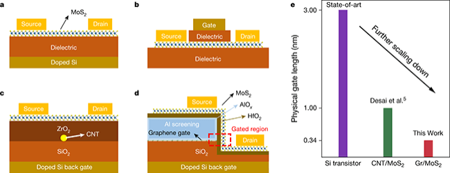
Researchers have recently demonstrated a new transistor design whose gate length is so small that it may be impossible to beat. The new device starts with a silicon substrate whose only purpose is to create a stepped edge foundation (it does not contribute to the electrical function of the transistor). This stepped edge then has an oxide layer deposited on top. Finally, a layer of molybdenum oxide is shrouded over the whole structure to create the final transistor with additional metal contacts for the source and drain. The action of the gate occurs along with the vertical structure of the step whereby the gate length is the height of the graphene layer adjacent to the semiconductor, one atom thick.

The new transistor structure (Image Source – Nature (Click to enlarge))
What makes the design of the new transistor potentially game-changing is that the researchers demonstrated multiple devices with success and that the construction method is easy enough to lead to mass production. By taking advantage of folding the monolayers on top of each other over an edge, the smallest gate length possible was achieved. This may see future designs consisting of tall structures with sheets folded over them to simultaneously create multiple channels.
Will atomic-scale devices ever be commercially feasible?
Even though the researchers here have demonstrated working devices with extremely small dimensions, there is no guarantee that it will be feasible from a commercial point of view. Even if researchers can make 1000 of these transistors side by side in a single manufacturing step, it doesn’t mean that 100 billion can be, and this is what matters most.
For the coming decades, it is more likely that SoP and SoM will become the popular technologies as they allow for stacked semiconductors with fast interconnects, which increases the total transistor count without having any noticeable effect on the dimension of the resulting chip. Furthermore, stacked technologies don’t require shrinking transistors to improve technology, and this is arguably far more economical than breaking the sub-nm barrier.

