Researchers develop a vertical colour sensor for even smaller cameras
| 26-04-2022 | By Robin Mitchell
Recently, researchers have created a vertically stacked colour sensor by taking advantage of van der Wall forces and believe that it could allow for the creation of simplified cameras. What challenges do current camera technologies face, what does the new sensor do, and how would it help with miniature camera technologies?
What challenges do current camera technologies face?
While camera technology has gone through leaps and bounds thanks to the ever-shrinking size of semiconductors and improvements in visual processors, engineers still face many challenges in the field of vision technology. The problems photographers faced in the 1970s using SLRs can still crop up in modern photography. Those trying to reduce the size of camera sensors will find that the physical nature of photons in the visual spectrum will not permit sensors that are too small.
To start, one problem that modern colour cameras face is a chromatic aberration which is the separation of light by colour. Simply put, a basic glass lens will show more aberration on the edges where the same image appears in different places at different wavelengths of light because the degree to which light rays are bent depends on their frequency. This means that modern cameras have to either use a series of complex heavy lenses to try and reduce this aberration or complex visual processors have to try and reduce the effect in post.
Another challenge presented to engineers is that photons of the visual spectrum have wavelengths between 400nm and 700nm, and this means that sensors detecting this light cannot be made smaller than this. Furthermore, traditional camera sensors will combine four sensors placed side by side in a grid to capture a single pixel, effectively quadrupling each pixel’s size. The use of four sensors comes from the need for separate sensors for each part of the spectrum (red, green, and blue), and the green spectrum gets two sensors instead of one (owing to the fact that the human eye is far more sensitive to green).
These challenges make it very difficult to create small cameras that can be mounted to miniature robotic devices. Basic lenses can help reduce the weight, but the overall image quality will be very poor. The reduction of camera sensors makes them less sensitive to light and thus struggle to work in low-light environments.
Researchers exploring the use of van der Wall semiconductors for future sensors
Recently, researchers from Georgia State University released a paper describing a new technique for creating sensors that can be made far smaller than those currently being manufactured. The new technique takes advantage of semiconductor layers that can be attached to each other via van der Wall forces which keeps them together but doesn’t allow them to electrically interact with each other.
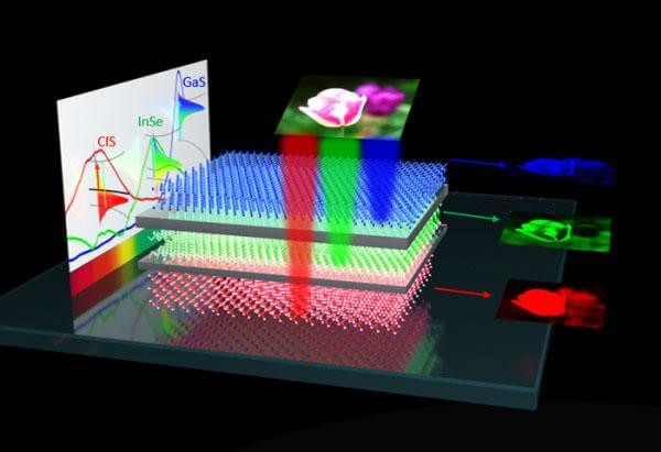
Each semiconductor layer is designed to absorb one of the three primary colour channels (red, green, and blue) while being transparent to other colour channels. These three layers are then stacked on top of each other, with van der Wall forces keeping them together. The resulting sensor is significantly smaller than commercial designs, which use four sensors alongside control transistors and other supporting circuitry. The three layers were manufactured from CIS, InSe, and GaS, with CIS being used to detect red frequencies, InSe for green frequencies, and GaS for blue frequencies. The development of the new sensor by the researchers has been done with the hope of creating visual-capable microminiature robotic systems for use in medical, environmental, manufacturing, and archaeology applications.

Camera sensor construction – Image courtesy Georgia State University
How would the proposed sensor help with miniaturising camera systems?
By far, the most significant advantage of the sensor developed by the Georgia State University researchers is that the vertical stacking of sensors allows for significantly increased pixel density. While this could translate to a camera sensor that is far more sensitive and physically larger (having more pixels in both axis), it is more likely that the sensor technology would allow for significantly smaller camera sensors.
The construction of a smaller sensor also allows for a smaller and simpler lens, but as we discussed earlier, a simpler lens can lead to chromatic aberration. However, the researchers of the new sensor noted that the use of a vertically stacked sensor with each pixel being located in the exact same location allows for corrective measures that can eliminate this effect. Therefore, smaller cameras are simpler to manufacture and will also be more cost-effective.
Thus, the new vertical sensor using van der Wall forces between layers will allow for cameras smaller than what is currently possible, and this will open the engineering field to using cameras on microminiature robotic systems. Additionally, the researchers also noted that the use of such sensors could be critical in restoring vision for the visually impaired as the sensor technology closely mimics the human eye in operation.
“This is a great step forward, but we are still facing scientific and technical challenges ahead, for example, wafer-scale integration. Commercial image sensors can integrate millions of pixels to deliver high-definition images, but this has not been implemented in our prototype yet. This large-scale van der Waals semiconductor device integration is currently a critical challenge to be surmounted by the entire research society. Along with our nationwide collaborators that is where our team is devoting our efforts.” – Dr Sidong Lei, Georgia State University.

