The Band Gap Showdown: GaN or SiC - Which Will Prevail?
Insights | 02-01-2024 | By Paul Whytock
Gallium nitride-enabled LED lighting is already making huge reductions to the amount of electrical power used globally, and in ten years’ time, it’s predicted that those savings could be as high as 46%.
But when it comes to the consumption of electricity, there is another electronics technology that could prove even more valuable in the crucial drive to cut global carbon emissions, and that’s power conversion.
Alongside the rise of GaN in lighting, advancements in packaging technologies for power electronics have been equally significant. The adoption of GaN and SiC necessitates innovative approaches to manage increased power capabilities. Recent developments in heatsink technology are particularly notable, playing a crucial role in maintaining the thermal performance of high-power devices and ensuring their reliability and efficiency across various applications.
Most people are totally unaware of how the technology of power conversion affects them, but this process happens many trillions of times a day globally and enables anything from mobile phones to electric vehicles to medical and industrial systems to function. In fact, any application where alternating electrical current has to be converted into direct current or the opposite. And because of inefficiencies in the electronic devices and systems that enable this process, a huge amount of Earth’s energy is wasted daily.

Emerging Technologies in Power Conversion
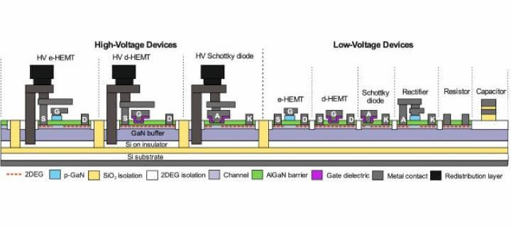
In the manufacturing of GaN and SiC, substrate choice is pivotal. While GaN-on-silicon leverages existing infrastructure and is typically limited to 650V, the advent of GaN-on-Qromis-substrate-technology (QST) allows for thicker epitaxial layers. This innovation enables operation at higher voltages, potentially up to 1,200V or more, thus expanding the scope of GaN and SiC in high-voltage power electronics applications.
It is fair to say there has been much progress electronically in reducing such power conversion inefficiencies thanks to the creation and implementation of various power electronics devices.
The impact of GaN technology extends beyond traditional power electronics, significantly influencing renewable energy systems. Known for high efficiency, GaN devices can substantially reduce the carbon footprint of systems like solar panels and wind farms, contributing to more sustainable and eco-friendly energy solutions in line with global environmental conservation efforts.
A key player in this has been the insulated gate bipolar transistor (IGBT). This device has served power conversion designs well and will continue to do so, particularly with legacy applications. But in the long term, advanced gallium nitride (GaN) and silicon carbide (SiC) semiconductor devices will be the way forward.
Transitioning to larger wafer diameters in the production of GaN and SiC introduces several challenges. Managing stress and adapting existing technologies for larger wafers are key hurdles. The strategic shift towards 8-inch fabs aims to harness the benefits of larger wafers but involves a complex and meticulous development process, underscoring the intricate nature of semiconductor manufacturing in the realm of advanced materials like GaN and SiC.
The Band Gap Factor
Both GaN and SiC belong to a class of devices called wide-bandgap semiconductors. The bandgap of a semiconductor is defined as the energy, in electron volts, needed for an electron to jump from the valence band to the conduction band. The valence band is simply the outermost electron orbit of an atom of any specific material that electrons occupy.
The energy difference between the highest occupied energy state of the valence band and the lowest unoccupied state of the conduction band is called the band gap and is indicative of the electrical conductivity of a material. A large band gap means a lot of energy is required to excite valence electrons to the conduction band. Conversely, when the valence band and conduction band overlap as they do in metals, electrons can readily jump between the two bands, meaning the material is classified as highly conductive.
The difference between conductors, insulators, and semiconductors can be shown by how large their band gap is. Insulators are characterised by a large band gap, so a large amount of energy is required to move electrons out of the valence band to form a current. Conductors have an overlap between the conduction and valence bands, so the valence electrons in such conductors are free.
However, semiconductors have a small band gap that permits a small amount of the valence electrons of the material to move into the conduction band. This property gives them a conductivity between conductors and insulators, which is part of the reason why they are ideal for circuits, as they will not cause a short circuit like a conductor.
Both GaN and SiC devices have already demonstrated enormous potential in increasing the efficiency levels of power conversion and thereby saving substantial amounts of electricity.
These two technologies have advantages over the other, and when these are considered, it currently looks like both will find a valued place in power conversion. But what are some of the differences?
The Fail Open Factor
SiC-based metal oxide semiconductor field effect transistors (MOSFETs) have the advantage of being fail-open devices.
![]()
This means that if a circuit fails, the device stops conducting current. This eliminates the possibility that a failure might lead to a short circuit and a possible fire or explosion. However, this beneficial and, at times, essential feature does mean its electrons are not as fast-moving, and this, unfortunately, increases resistance, which is the main enemy of efficient power conversions.
Enter GaN-based devices that do have high electron mobility. GaN transistors are different because most of the current flowing through the device is due to electron velocity rather than charge amount. This means the charge has to enter the device to switch it on or off. That cuts the energy needed for each switching cycle and delivers a more efficient power conversion operation.
But rather than seeing one particular technology as a winner, it must be remembered that sometimes the different operational characteristics and subsequent advantages of both GaN and SiC can be beneficial in certain applications.
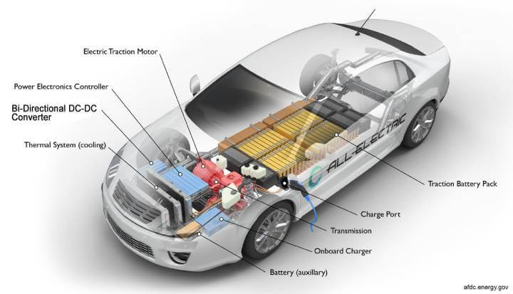
Let’s take a look at the car makers and their choices when it comes to wide bandgap decisions relative to electric vehicle (EV) designs, and in particular, the work the vehicle’s inverter does, which is fundamentally power conversion.

EVs need an inverter to convert DC current from the lithium battery to AC current that the vehicle's electric motor can use. Suppliers of SiC devices were Elon Musk's choice for his Tesla cars, and now Chinese vehicle manufacturers BYD, Toyota, Hyundai, and Mercedes have followed suit.
However, SiC devices do not have it all their own way when it comes to car makers.
The higher switching speeds possible with GaN are a powerful advantage in EV inverters because they use hard-switching. This enhances performance by switching rapidly from on to off to cut the time the device is holding high voltage and passing high current.

Besides an inverter, an EV also typically has an onboard charger, which enables the vehicle to be charged from a mains current by converting AC to DC. Here again, GaN is very attractive.
Several challenges come with using SiC in automotive applications. SiC substrates don’t come cheap and makeup nearly 50% of the cost of the bill of materials to produce the device. SiC is also inherently a low-yield manufacturing process, and the wafer is transparent, necessitating costly metrology equipment to monitor the process.
Making SiC devices is more difficult than manufacturing Si-based semiconductors, and the hardness of SiC makes etching and gate oxide processes difficult.
When it comes to vehicle manufacturing, car makers need high volumes of supplied products to keep production lines flowing, and here, the supply of SiC is limited, which is another obstacle to its adoption in the automotive industry.
In comparison to SiC, GaN is grown on a less expensive Si substrate. However, they do need a larger die size for high-current applications compared to SiC.
Component Reliability Paranoia
The use of Si substrates can sometimes cause problems like lattice mismatch and dislocations, which in turn cause gate-current leakage and lower reliability, and carmakers are paranoid about component reliability as operational failures escalate car warranty returns and subsequently bite a chunk out of the carmaker’s profits.
Admittedly, these problems with GaN could easily be resolved by beefier epitaxy layers, but that, in turn, would increase the overall component cost, and once again, the car makers are hyper-cost-conscious when it comes to the price of supplied components.
Creating suitable semiconductor devices for automotive use always has to address temperature considerations, and because GaN is grown on a Si substrate, its thermal conductivity is subject to how Si substrates perform.
GaN does have limitations for high-power automotive applications (above 10 kW) and is preferred for devices below 600V, but it does have the potential to enter the inverter market with multi-level power topology. As car makers need ever-increasing amounts of power for features like infotainment, fast communication, cameras and radar, there is an increasing interest in 48V systems. In this aspect, GaN is suitable because it is cost-competitive.
Future Prospects in Power Electronics
As mentioned earlier, GaN enables system-level cost savings. Device and system costs depend on substrate cost, wafer fabrication, packaging and overall yield in the manufacturing process.
SiC and GaN serve different voltage, power and application needs. SiC handles voltage levels up to 1,200V with high current-carrying capabilities. This makes them suitable for applications in automotive inverters and solar farms.
Alternatively, because of its switching capabilities at high frequencies and its cost advantages, GaN has become the device of choice for many designers in <10-kW applications.
So those are just some of the operational differences between the two bandgap technologies, and answering the headline question of which will be the overall winner is impossible at this stage, primarily because both are constantly evolving in terms of performance.
Looking to the future, the power electronics industry is eyeing emerging materials like gallium oxide (Ga2O3). While Ga2O3 holds promising potential, its adoption will be gradual, given the industry's conservative nature. The widespread acceptance and application of these novel materials in high-power scenarios will hinge on their ability to establish a proven track record.
When it comes to GaN, it has the capability to provide very fast switching while simultaneously operating at high temperatures. It also has size advantages, is considered to have a low carbon footprint, and is very reasonable in terms of manufacturing cost.
From the SiC perspective, things are looking good for the makers of these devices when it comes to the electric vehicle market.
According to consultancy company McKinsey, 800V battery electric vehicles (BEVs) are most likely to use SiC-based inverters because of their high efficiencies, and it is expected that by the end of the decade, BEVs will account for 75% of the electric vehicle market.
Putting aside the technical variations between the two technologies, what do the analysts and pundits say about how well they will sell for the rest of this decade?
Taking an average from a cross-section of industry pundit views, it seems SiC will do well, and sales will achieve a compound annual growth rate (CAGR) of 29% and reach a global figure of € 12 billion by 2030.
The financial picture looks just as rosy for GaN device sales. Although the CAGR figures amongst market analysts tend to have a wider variation, the overall average figure pans out at 26%, and sales should reach approximately €10billion by 2030.
So, in terms of technical competence, application versatility and the ability to make the semiconductor companies a lot of money, there’s not much to separate GaN and Sic, and so perhaps if there is to be an eventual winner of the bandgap race, it will depend on which of them can demonstrate the most disruptive technology.

