Chinese Ultra-Thin Semiconductor Method May Boost Microchip Speed
Insights | 20-08-2024 | By Robin Mitchell
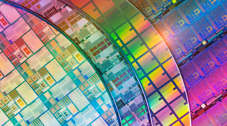
The innovative method developed by researchers in China for creating ultra-thin semiconductors has the potential to z the landscape of microchip technology. By enabling the production of semiconductor layers just a few atoms thick, this breakthrough promises faster and more energy-efficient microchips, essential for powering a variety of electronic devices. Utilising molecular beam epitaxy (MBE), the researchers have demonstrated superior performance of these ultra-thin semiconductors compared to traditional thicker ones. As the team continues to enhance their technique and delve into commercial applications, the following questions arise.
What challenges do semiconductors face with regard to speed, what specific advantages do ultra-thin semiconductors offer in terms of speed and power consumption over their thicker counterparts, and in what ways might this advancement impact the future development of electronic devices?
Key Things to Know:
- Innovative Approach to Semiconductor Production: Chinese researchers have developed a novel technique to create ultra-thin semiconductors just a few atoms thick, leading to significant improvements in performance and a reduction in defects in microchips.
- Scalable Production Capabilities: The new method enables the production of up to 15,000 semiconductor layers at a rate of 50 layers per minute, paving the way for mass production and widespread adoption in various high-demand technologies.
- Enhanced Performance and Efficiency: These ultra-thin semiconductors offer superior electron mobility and lower power consumption, making them ideal for next-generation integrated circuits, particularly in mobile devices, data centres, and AI systems.
- Strategic Impact on Global Semiconductor Industry: The successful development and scalability of these semiconductors could position China as a leader in the global semiconductor market, with significant implications for the future of electronics and technological innovation.
The Hurdles of Achieving Higher Semiconductor Speeds
As the need for faster computational devices increased, engineers faced a multitude of challenges that hindered the development of speedy semiconductors. One of the primary obstacles was finding materials that could be made smaller to reduce the size of electronic components, as smaller parts operate faster due to reduced physical distances. However, this came with the added challenge of ensuring that these materials could maintain their electrical and thermal properties, as devices of the future would need to integrate on extremely small scales.
The quest for fast semiconductors also led to the advancement of new computing architectures and circuit topologies. Engineers explored the use of parallel processing, pipelined designs, and high-speed digital signals to boost the speed of devices, but this came with the challenge of increased power consumption and reduced efficiency. Thus, engineers had to strive to find a delicate balance between speed and energy efficiency, employing innovative techniques to optimise their designs for faster performance without sacrificing energy resources.
However, this pursuit of faster performance in semiconductor technology is fraught with numerous challenges that continue to plague researchers today. To start, the physical limitations and technical constraints make it difficult for engineers to develop even faster semiconductors. The industry's reliance on traditional materials and manufacturing processes also restricts further miniaturisation and efficiency enhancement, leading to stagnation and impeding progress towards achieving faster speeds.
The trade-off between speed and power consumption is a major hurdle, as higher speeds require increased chip density, resulting in higher energy consumption and heat generation. This power consumption issue not only reduces the lifespan of semiconductor devices but also poses a major challenge for engineers in enhancing speed capabilities.
The historical evolution of semiconductors, from vacuum tubes to silicon-based chips, highlights the long journey towards improving speed capabilities. However, the current speed limitations faced by semiconductors cast a shadow over future prospects, making it a challenging task to achieve greater speeds.
The Future of Microchip Technology
The introduction of ultra-thin semiconductors that are only a few atoms thick has the potential to reshape the landscape of microchip technology. By enabling the production of semiconductor layers that are significantly thinner than their traditional counterparts, researchers in China have opened up new possibilities for creating faster and more energy-efficient microchips that are essential for powering a wide range of electronic devices.
One of the most remarkable aspects of this development is the method employed by the researchers, which circumvents the traditional limitations of crystal growth. By utilising the "grow at interface" technique, the team was able to maintain a high level of structural control, ensuring that each atomic layer is perfectly aligned. This precision not only enhances the performance of the resulting semiconductors but also significantly reduces the occurrence of defects, which are often the bane of semiconductor manufacturing.
Advancements in Ultra-Thin Semiconductor Technology
The use of molecular beam epitaxy in the production process has also led to superior performance compared to traditional methods, setting the stage for a new era in semiconductor manufacturing. The implications of this breakthrough are significant, with the potential to transform the capabilities of microchips and enable them to meet the growing demands of modern electronic devices. The ultra-thin semiconductors developed by the researchers mark a significant advancement in the field of microchip technology, paving the way for further innovation and progress in the industry.
Additionally, the scalability of this technique is noteworthy. With the ability to produce up to 15,000 layers at a rate of 50 layers per minute, this method opens the door to mass production of ultra-thin semiconductors. This is a crucial step forward, as it addresses the industry’s need for both quality and quantity, ensuring that these advanced materials can be produced efficiently and at scale, which is essential for widespread adoption in various technological applications.
The implications of this technological breakthrough are vast. The enhanced electron mobility and reduced power consumption of these ultra-thin semiconductors make them ideal candidates for next-generation integrated circuits. As these materials meet and even exceed international standards for chip performance, they position themselves as a formidable alternative to traditional silicon-based semiconductors, particularly in high-demand sectors such as mobile devices, data centres, and advanced AI systems.
The Future of Electronics Has Only Just Begun
With the potential to enhance device performance significantly, these ultra-thin semiconductors could lead to faster processing speeds and reduced power consumption, resulting in electronic devices that offer improved efficiency. This advancement could also translate to longer battery life and a better user experience, setting a new benchmark for future smartphones, laptops, and other gadgets.
As the use of ultra-thin semiconductors becomes widespread, it is likely to influence industry standards, with companies needing to adapt their manufacturing and design processes to incorporate these advanced components. This shift could lead to a new era of innovation and competition in the market, with engineers and researchers exploring new applications for these thin semiconductors.
Looking ahead, the adoption of ultra-thin semiconductors is poised to drive long-term technological advancements, with researchers already exploring the potential of these components in medical devices and advanced artificial intelligence systems. The possibilities are vast, and the future holds promise for the Chinese method of producing ultra-thin semiconductors to become a game-changer in the technology industry.
