Advanced IC Packaging and Its Role in the Chip Wars
Insights | 17-09-2024 | By Robin Mitchell
The race for superior IC packaging technologies is heating up in the global semiconductor industry, with a focus on integrating more components into smaller packages to meet the demand for high-performance electronic devices. As countries and companies invest significantly in research and development, the competition intensifies, shaping the landscape of technological leadership worldwide.
Key Things to Know:
- China is leveraging advanced IC packaging technologies, including 2.5-D and 3-D stacking, to overcome US sanctions and maintain competitiveness in the global semiconductor market.
- Fan-out wafer-level packaging (FOWLP) is helping Chinese manufacturers reduce chip sizes while enhancing performance, particularly for high-performance computing and mobile applications.
- Silicon interposers and hybrid bonding technologies are enabling faster data transfer and improved power efficiency, crucial for AI and 5G advancements.
- The global semiconductor landscape is evolving as advanced packaging techniques drive innovation, pushing the boundaries of technology and redefining competition in the industry.
How do advanced IC packaging technologies contribute to the performance and functionality of electronic devices, what specific techniques are being employed to achieve integration of more components into smaller packages, and how might the developments in IC packaging impact the future of electronics?
The Evolution of IC Packaging Technologies: From Chiplets to Advanced Die-to-Die Designs
The historical evolution of IC packaging methods has been marked by a gradual shift towards more advanced techniques, promising improved performance, efficiency, and reliability of electronic devices. However, the reality often falls short of expectations, and the transition to advanced IC packaging has posed numerous challenges and complexities that hinder the seamless integration of these technologies into electronic devices.
Despite the potential for enhanced speed and efficiency, the implementation of advanced IC packaging techniques does not always translate into significant performance improvements due to thermal management, signal integrity, and power distribution issues that limit the full potential of these technologies.
The introduction of advanced IC packaging has also been accompanied by complexities that arise from the design and manufacture of complex packaging structures, leading to challenges in integrating multiple functionalities within devices. The intricacies of optimising packaging solutions for real-world applications and ensuring compatibility, scalability, and cost-effectiveness pose significant hurdles in the practical implementation of advanced IC packaging technologies.
The rapid pace of innovation in the semiconductor industry has further raised concerns about the long-term viability of advanced IC packaging technologies, leading to a fragmentation of competing technologies and raising questions about interoperability and standardisation. As the industry navigates these challenges, the true impact of advanced IC packaging on device design and consumer expectations remains a complex and evolving landscape. The journey towards leveraging the full potential of advanced packaging techniques is riddled with obstacles that can dampen initial enthusiasm for these innovations.
The Semiconductor Industry Enters a New Chapter: Advanced IC Packaging Technologies in the Chip Wars
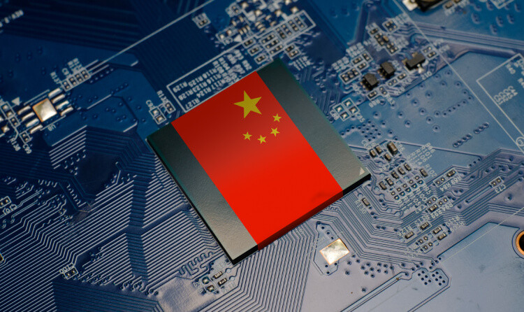
The global semiconductor industry is witnessing a surge in the race for superior IC packaging technologies as countries and companies invest significantly in research and development to meet the growing demand for high-performance electronic devices. The competition is shaping the landscape of technological leadership worldwide, with China leveraging advanced design and packaging technologies to overcome US sanctions that have restricted its access to high-end AI processors. By focusing on innovative IC packaging solutions, China aims to enhance its semiconductor capabilities and strengthen its position in the global market.
In particular, China's focus on 2.5-D and 3-D packaging techniques has allowed for more compact, efficient designs that support next-generation applications such as AI and edge computing. By leveraging these advanced packaging technologies, Chinese semiconductor manufacturers can stack multiple chips within a single package, significantly enhancing data transfer rates and computational performance. This strategic use of advanced die-to-die integration allows China to remain competitive in the high-performance computing market, despite restrictions on advanced processor technologies.
Leveraging Advanced Packaging to Overcome Sanctions and Drive Innovation
The integration of advanced IC packaging technologies not only enables China to mitigate the impact of sanctions but also drives the development of more efficient and powerful electronic devices. By optimising the packaging of integrated circuits, China can enhance the performance and functionality of its semiconductor products, catering to the increasing demand for high-performance electronics in various industries. The emphasis on design and packaging tech advances underscores China's strategic vision to establish itself as a key player in the semiconductor industry and its commitment to technological innovation and competitiveness on a global scale.
The development of fan-out wafer-level packaging (FOWLP) has further bolstered China's semiconductor capabilities. By utilising this technology, Chinese manufacturers are able to increase input/output density and reduce the overall size of their chips, making them ideal for applications in mobile devices, automotive systems, and high-performance computing. As China continues to refine its FOWLP processes, it positions itself to dominate key segments of the semiconductor market that require high-performance, low-power chips.
The utilisation of advanced IC packaging technologies by China signifies a significant shift in the dynamics of the chip wars, where packaging innovations play a crucial role in determining the performance and efficiency of electronic devices. As China continues to make strides in developing and implementing advanced packaging solutions, the competition in the semiconductor industry intensifies, driving further advancements and pushing the boundaries of technological capabilities.
China’s Strategic Use of Silicon Interposers to Enhance Semiconductor Competitiveness
Additionally, China's integration of silicon interposers in advanced IC packaging enables the combination of multiple functional components, such as logic and memory chips, into a single package. This approach allows for faster data transfer and improved power efficiency, which are critical for emerging technologies like AI and 5G. The use of advanced interposer technologies, such as TSMC’s CoWoS and Intel's EMIB, demonstrates China's ability to stay at the forefront of packaging innovations, contributing to its competitive edge in the global semiconductor race.
China's proactive approach to investing in advanced IC packaging technologies reflects its determination to achieve technological self-reliance and overcome the limitations imposed by trade restrictions. By positioning itself as a formidable player in the global semiconductor arena, China is ultimately aiming to bridge the gap in advanced electronics and secure its access to cutting-edge technologies. The semiconductor industry is entering a new chapter in the ongoing chip wars, where innovation and efficiency will be key drivers of success.
Furthermore, China's investments in hybrid bonding technologies, which enable a seamless connection between stacked chips without traditional solder bumps, provide a critical advantage in reducing the space and power requirements of advanced semiconductor devices. This technology, still in its nascent stages globally, is set to become a game changer in producing more powerful, energy-efficient chips that meet the demands of AI, autonomous vehicles, and other high-tech industries.
The Future of Electronics: Advancements in IC Packaging and Its Impact on Competition, Innovation, and Technology
The landscape of integrated circuit packaging is experiencing a significant transformation as technology advances, with developments set to greatly shape the future of electronics. The evolution of IC packaging is not merely a technical advancement but a strategic move that will have far-reaching implications across various sectors, redefining competitive dynamics in the semiconductor market and leading to significant market shifts.
Companies will adapt to these innovations to meet the evolving demands of consumers, and the focus on innovation and research and development in IC packaging will intensify as companies seek to capitalise on the potential of these advancements. Engineers and researchers will concentrate their efforts on exploring new possibilities, pushing the boundaries of what is currently achievable, and driving breakthroughs in IC packaging, leading to a wave of innovative solutions that will shape the future of electronics.
The impact of these packaging innovations extends beyond the semiconductor industry, having broader implications for electronics engineering as a whole. Engineers will benefit significantly from these advancements, gaining access to cutting-edge packaging technologies that will streamline the design and development process of electronic devices. By leveraging these innovations, engineers will be empowered to create more efficient, compact, and powerful electronic systems that cater to the evolving needs of consumers.
The future of electronics engineering is poised to be transformed by the advancements in IC packaging, ushering in a new era of possibilities where engineers have access to a diverse range of packaging solutions that enable them to push the boundaries of innovation. As a result, we can expect to see a proliferation of next-generation electronic devices that are more advanced, energy-efficient, and compact.
