Intel 18A Node Explained: How RibbonFET Boosts AI Scalability
Insights | 18-10-2024 | By Matthew Walker
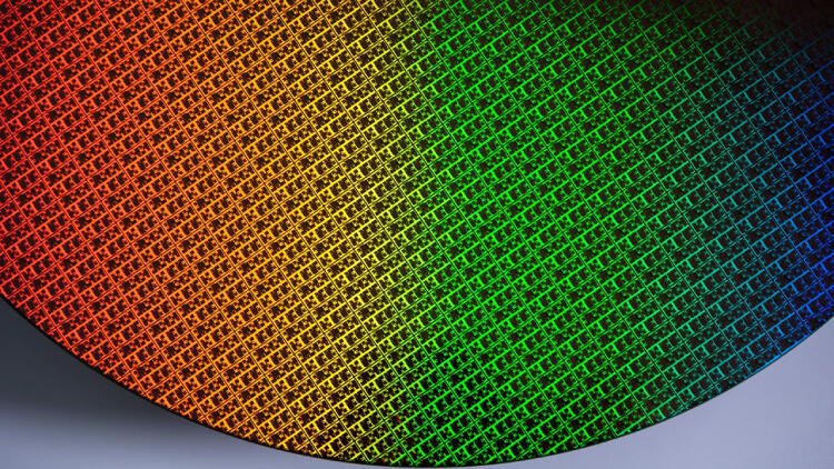
Intel 18A, the cutting-edge process node from Intel Foundry, is set for production by 2025. Featuring RibbonFET and PowerVia, it will enable foundry clients to achieve higher processor scalability and efficiency, accelerating advancements in AI computing. (Credit: Intel Foundry)
Intel's 18A node is one of the most significant advancements in chip technology since FinFET was introduced in 2011. As part of Intel's aggressive 5 Nodes in 4 Years (5N4Y) roadmap, it aims to reestablish Intel as a leader in semiconductor manufacturing. With innovations like RibbonFET and PowerVia, Intel is transforming the way transistors and power are delivered within chips.
Here are the key things to know about Intel 18A:
- RibbonFET is Intel's first Gate-All-Around (GAA) transistor, offering up to 15% better performance per watt compared to FinFET
- PowerVia is the industry's first backside power delivery technology, improving cell utilisation by 5-10% and boosting ISO-power performance by 4%
- Intel 18A is designed for high-performance computing (HPC) and mobile applications, where power efficiency and performance are critical
- Part of Intel's roadmap to compete with TSMC and Samsung, this node will help Intel leapfrog the competition in the 3nm and 2nm process space
Overview of Intel's 5 Nodes in 4 Years Strategy
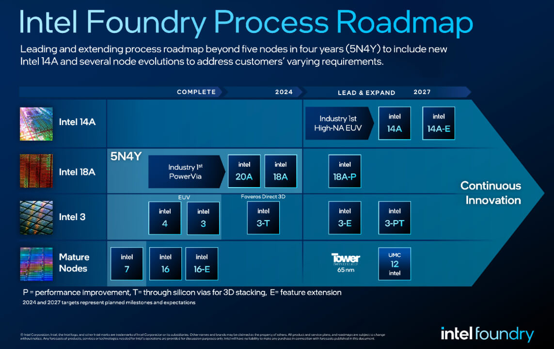
Intel's 5 Nodes in 4 Years (5N4Y) strategy is a highly aggressive roadmap announced in 2021, aimed at regaining leadership in the semiconductor industry. The goal is to deliver five new process nodes in just four years, a pace much faster than the industry norm. This plan includes several process node innovations from Intel 7 to Intel 18A, focusing on pushing the limits of transistor density, performance, and energy efficiency.
Key Nodes: Intel 7, 4, 3, 20A, and 18A
- Intel 7: This node, launched in 2021, uses deep ultraviolet lithography (DUV) and serves as the foundation for Intel's Alder Lake and Raptor Lake processors
- Intel 4: Intel's first node to use extreme ultraviolet lithography (EUV), delivering a significant leap in transistor density and power efficiency compared to Intel 7
- Intel 3: A refinement of Intel 4, with 18% better performance per watt, but primarily aimed at data centers.
- Intel 20A: This node introduces the RibbonFET transistor and PowerVia backside power delivery technology. The "A" stands for angstrom (0.1 nanometers), indicating the transition to atomic-scale technology.
- Intel 18A: The most advanced of these nodes, expected in mid-2024, will further optimise RibbonFET and PowerVia, offering up to 15% better performance per watt over Intel 20A.
The Role of Intel 18A in This Timeline
Intel 18A is critical because it's the node that is expected to bring Intel back to process leadership by 2025. It builds on the innovations of Intel 20A but focuses on further improving transistor density and power efficiency. By optimising RibbonFET and PowerVia, Intel aims to deliver chips that outperform competitors like TSMC and Samsung in terms of performance per watt and transistor scaling.
 Source: Intel
How TSMC and Samsung Compare with Intel's Process Roadmap
Currently, TSMC and Samsung lead in advanced semiconductor manufacturing, with TSMC's 3nm process already in production and Samsung pushing its GAAFET technology with 3nm. These companies have maintained a lead over Intel for several years, particularly in the race to master extreme ultraviolet (EUV) lithography.
- TSMC: Their 3nm process is already in production, with plans for 2nm by 2025, featuring their own take on Gate-All-Around (GAA) technology.
- Samsung: The first to implement GAAFET with its 3nm 3GAE process, but struggling with yield issues.
Intel's Plan to Leapfrog Competitors Using RibbonFET and PowerVia
Intel is betting on RibbonFET and PowerVia to regain its competitive edge. By transitioning from FinFET to GAA transistors with RibbonFET, Intel improves both density and performance per watt, something TSMC is expected to achieve only with its 2nm node in 2025.
Additionally, PowerVia, Intel's backside power delivery technology, gives it a unique advantage by separating power and signal pathways, reducing congestion and boosting performance efficiency. TSMC and Samsung have yet to introduce similar backside power delivery technologies, putting Intel in a strong position for when 18A becomes widely available.
Breaking Down Intel 18A Technology
What is RibbonFET?: Intel's Gate-All-Around (GAA) Transistor
RibbonFET is Intel's version of a Gate-All-Around (GAA) transistor, representing a significant evolution in transistor design. GAA transistors wrap the gate around the channel, offering more precise control of the current flow compared to the older FinFET architecture, where the gate only touches three sides of the channel. RibbonFET allows current to flow through stacked "ribbons," hence its name, which leads to increased transistor density and power efficiency.
Comparison to FinFET: How RibbonFET Enhances Density and Power Efficiency
Compared to the FinFET architecture that Intel pioneered in 2011, RibbonFET significantly improves performance per watt and enables better scaling for smaller nodes. In simple terms, FinFET allowed for three-dimensional control over current flow, but RibbonFET takes this further by wrapping the gate completely around the channel, creating a four-sided control over current.
- Higher density: More transistors can be packed into the same area, which is a critical need as we approach the Angstrom scale in chip design.
- Better power efficiency: The improved control reduces leakage current, meaning less power is wasted, making it ideal for mobile devices where battery efficiency is a priority.
Advantages for HPC and Mobile Devices
The benefits of RibbonFET extend beyond just density. For high-performance computing (HPC) applications, this architecture provides the power and scalability required to handle AI workloads and massive data processing, all while maintaining lower power consumption. For mobile devices, RibbonFET's ability to reduce power consumption directly translates into longer battery life and more powerful smartphones without generating excessive heat.
How RibbonFET Improves Performance per Watt by up to 15%
Intel has indicated that the move to RibbonFET will boost performance per watt by up to 15% compared to the previous FinFET nodes like Intel 4. This performance boost is essential for driving next-generation AI, cloud computing, and 5G applications, where power efficiency is as important as processing speed.
PowerVia: A New Approach to Power Delivery
PowerVia is Intel's innovative backside power delivery network (BS-PDN), the first of its kind in the industry. Traditionally, both power and signal wires have been routed on the front side of the chip, which creates congestion and limits performance. PowerVia separates these functions, moving the power delivery to the back of the chip and leaving more space for signal wiring on the front. This breakthrough increases both performance and chip design flexibility, as power no longer competes for routing space with signals.
How Backside Power Delivery Frees Up Space and Improves Performance
PowerVia's most significant advantage is the ability to reduce congestion on the chip by moving power delivery to the back. This allows more room for signal routing on the front side, leading to:
- 5-10% better cell utilisation: With more efficient use of space, chips can pack more transistors into the same area, improving both performance and power efficiency.
- 4% ISO-power performance improvement: Intel reports a 4% improvement in ISO-power performance, meaning that devices can achieve higher performance at the same power consumption levels.
Intel's recent research is shaping the future of transistor technology. By advancing 3D stacked CMOS transistors and backside power delivery methods like PowerVia, Intel is extending Moore’s Law well beyond current expectations. These innovations, closely tied to Intel 18A, are driving improvements in transistor density and power efficiency, ensuring Intel stays competitive in the high-performance computing space. For a deeper dive, watch the video below, which explains how these advancements contribute to the 18A node's success.
Implications for Future Chip Designs
PowerVia is set to become a cornerstone of Intel's future process nodes, particularly in Intel 20A and Intel 18A. The technology will be especially beneficial for high-performance computing and mobile processors, where both power efficiency and chip size are critical. Furthermore, as backside power delivery becomes more widespread, it could allow Intel to lead the way in creating smaller, faster, and more efficient devices, outpacing competitors like TSMC and Samsung, which are expected to adopt similar technologies only by 2025-2027.
Applications of Intel 18A in High-Performance Computing and Mobile
High-Performance Computing (HPC)
Intel 18A is highly optimised for high-performance computing (HPC) environments like data centers and AI applications, which require immense processing power, scalability, and energy efficiency. The introduction of RibbonFET and PowerVia in Intel 18A addresses the need for both high-density and high-efficiency transistors. This is particularly crucial in data centers that run AI workloads, as these systems need to manage vast amounts of data while minimising power consumption and cooling costs.
The architecture is especially well-suited for AI-driven tasks like machine learning, big data processing, and cloud computing, where low latency and high throughput are essential.
By delivering up to 15% better performance per watt, Intel 18A is poised to handle more operations in parallel, which is crucial for tasks involving deep learning algorithms and neural networks that require vast computational resources.
Examples of Key Applications: AI Workloads, Big Data Processing, and Cloud Computing
- AI Workloads: Intel 18A's architecture will accelerate training and inference in deep learning models by maximising processing efficiency and minimising latency.
- Big Data Processing: RibbonFET's enhanced density is crucial for handling massive datasets. This will allow companies running big data analytics to process information faster and more efficiently.
- Cloud Computing: As cloud services demand higher efficiency and more power-per-watt, Intel 18A's PowerVia technology will enable cloud platforms to support more users and applications without increasing energy consumption
Mobile Applications
Intel 18A's RibbonFET and PowerVia technologies are also game-changers for the mobile sector. With mobile devices, battery life and thermal efficiency are critical concerns, especially as smartphones and tablets become more powerful. RibbonFET's ability to reduce power leakage significantly improves power efficiency, directly leading to longer battery life.
Future Outlook: Beyond Intel 18A, What Comes Next?
Following Intel 18A, the company's roadmap doesn't slow down. Intel 14A is the next major node on the horizon, projected to build on the advances introduced by 18A. With Intel 14A, the company will continue to refine both RibbonFET and PowerVia technologies, integrating further transistor-level and packaging innovations.
This node is expected to feature second-generation implementations of both RibbonFET and PowerVia, leading to even better efficiency and performance, while introducing High NA EUV (High Numerical Aperture Extreme Ultraviolet lithography), which enables even smaller feature sizes.
In addition to Intel 14A, specialised node evolutions like Intel 3-PT are set to introduce advanced 3D packaging technologies, leveraging through-silicon vias (TSVs) for enhanced performance in complex designs.
TSVs enable more efficient vertical connections between layers of silicon in 3D chips, leading to better power efficiency and higher performance, especially for heterogeneous computing and AI-driven applications.
Challenges and Competitors
While Intel is advancing rapidly, TSMC and Samsung remain fierce competitors. TSMC's 2nm node is expected to enter production around 2025, utilising their own version of Gate-All-Around (GAA) transistors, which will be crucial for AI, mobile, and HPC applications. Samsung has already moved to 3nm GAA transistors and is pushing toward 2nm with improved yields.
Both companies have an edge in terms of foundry market share and customer base, particularly for fabless chipmakers like Apple, AMD, and Qualcomm. As they scale up their 2nm nodes, Intel faces stiff competition in both technological advances and customer acquisition.
The Potential for Intel to Regain Market Leadership
Intel's potential to regain market leadership hinges on the successful execution of Intel 18A and Intel 14A, along with innovations like PowerVia and RibbonFET. These breakthroughs could enable Intel to outperform TSMC and Samsung in power efficiency and performance per watt. Furthermore, Intel's commitment to internal production and foundry services (via Intel Foundry Services, or IFS) aims to attract external customers, positioning Intel as a more attractive option for fabless companies in the coming years.
If Intel can maintain this momentum, it will stand a strong chance of narrowing the gap between TSMC and Samsung, especially as it introduces its advanced packaging solutions like TSVs and continues its work on 3D chips.