Designing for (Issue Free) Manufacture: ‘Not My Problem’, or Should It Be?
Insights | 04-03-2025 | By Rory Dear
The separation of the PCB design and manufacturing functions is typical in most OEMs, where PCB assembly is outsourced rather than undertaken internally. Outside of especially large OEMs, it rarely makes financial sense to invest in and maintain an expensive internal SMT line and everything that goes with it. So an EMS like DSL electronic manufacture is typically contracted to undertake that PCB assembly.
With that separation, the communication lines are less clear than when design and manufacturing both take place under the same roof and even with the best will in the world, sometimes they are purposefully muddied purely by trying to do the right thing by a client.
For decades, my business only sat on one side of that fence. We were exclusively PCB designers and used EMS/CEMs ourselves, outsourcing the manufacture of PCB designs we’d undertaken for our client base. Our carefully selected EMS undoubtedly did a great job, they produced our designs hassle free and without complaints – but we’ve only realized since launching our own manufacturing service this wasn’t necessarily in our best interests.
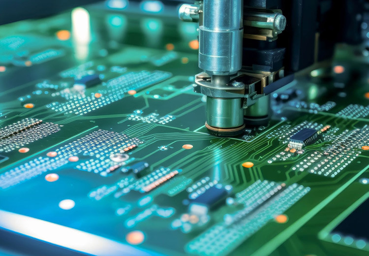
To explain why, we must jump to the other side of the fence, and look through the lens of us functioning as purely a manufacturer of an externally designed PCB. There is a huge range in the quality of the manufacturing data pack and the manufacturability of the PCB design that an EMS receives on a day to day basis.
Manufacturing pack
The manufacturing pack in the world of PCB assembly is effectively the same ‘brief’ and scope detail almost every conceivable business receives as its first input into a new opportunity. Whether you’re architects, caterers, event organizers or even contract cleaners, the brief can either be crystal clear, or clear as mud.
At their worst, we’ve seen manufacturing packs with
- Manufacturer part numbers that don’t exist
- PCB footprints that don’t match the component footprint
- BOM parts that aren’t in the PCB design (or vice versa)
- Revision numbers that don’t match up
- No Pick and Place data (so no indication of where to put X component)
Most EMS/CEMs, including ourselves, do understand that there are circumstances where this is unavoidable, perhaps their designer left to pastures new and thus they need this support to resolve these issues. Typically an EMS, as we are, are always happy to help, but it does delay the quoting process and as manufacturing builds are often urgent – this inevitably adds days before we can even quote the build, let alone start it.
PCB Design
Prior to launching our own manufacturing service, our internal PCB designers, no doubt motivated by our ‘embedded’ credentials would always design every PCB to be as ‘small as possible’, using the smallest pads, smallest courtyards and smallest everything to shrink that circuit into the smallest overall area possible. If that made manufacturing more difficult…not our problem.
Developing an electronic product typically involves hardware and software. Simplistically, a lone hardware engineer prefers simple hardware, even at the expense of more complex software; whereas a lone software engineer prefers simpler software coding, even at the expense of more complex hardware. Finding that compromise to serve both sides of the fence is a regular consideration when designing an electronic product.
There are many considerations synonymous to this in PCB design vs PCB manufacturing, a simple one to consider is pad size.
A PCB designer wants as small pads as possible and as hidden as possible, to maximize space and reduce the size of a PCB design where possible. Sometimes this is to fit in a defined space, thus necessary, others it’s a preference for a smaller PCB with more layers, which incidentally isn’t always more cost-effective these days. Smaller pads can also reduce EMC levels so are often preferred.
A PCB manufacturer effectively wants as large pads as possible and as exposed as possible, to make solder flow and rework easier, plus make it easier to inspect said solder joints via automated optical inspection (AOI) or by eye.
This is just one area of consideration amongst many that have dependencies upon each other or can conflict.
The blind designer
As we’ve seen historically, the reality is that beyond Design-For-Manufacture (DFM) training that open communication line of manufacturers helping designers produce more easily manufacturable PCBs, thus with faster quoting, builds and yield simply doesn’t happen. Manufacturers often don’t want to be coming to their clients with ‘problems’ when if it would reduce the unit cost, lead time or yield of a PCB design – surely the designers would want to know that?
The blind manufacturer
Unlike DSL electronic manufacture, many EMS companies simply don’t have in-house engineering expertise, they are exclusively manufacturers so will rigidly and blindly build exactly what your manufacturing pack tells them to and if it doesn’t work, or there’s any issues, that’s a “you problem”. Thankfully most EMS companies have realized that it’s in no one’s interest for a build to fail, no matter who’s ‘fault’ it is. For DSL electronic manufacture, 100% working product is particularly important as we don’t charge any NRE, so the cost of having to create a new stencil, for example, falls on us.
Supporting PCB Design for (issue free) manufacture
Some designers have had career exposure to the manufacturing side, thus will already understand many of the factors that make a PCB easier (thus lower cost, faster lead time and higher yield) to manufacture – but many haven’t.
To mitigate this and to allow our clients exposure to that knowledge that we’ve gained, we do this in the form of a free of charge Design Health Check.
Whether you’re building a long established design, or an entirely new prototype, we’ll run your PCB design by both our electronic design and manufacturing teams to get their professional opinion on any evident issues, or manufacturability improvements you could make. After all, a more manufacturable design benefits everyone.