Miniature sensor developed for tracking butterfly migration
05-05-2022 | By Robin Mitchell
Recently, researchers have created a sensor that can track environmental factors such as light and temperature, whose small size and weight allow it to be mounted on the back of a butterfly. Why are researchers interested in butterflies, what did the researchers develop, and how does the use of stacked ICs show their great advantages?
Why are researchers interested in butterflies?
Like all other lifeforms on earth, butterflies play a crucial role in the food chain, preying on pests that often threaten plants while simultaneously acting as pollinators. Of course, butterflies also play a role in plant destruction when in their caterpillar form (mainly towards the Brassica family, such as cabbage and broccoli), which is why vegetable enthusiasts will often use pesticides against them. But, for those with flower gardens and natural habitats, butterflies are an excellent insect to attract, even if just for their aesthetic appeal.
However, some butterflies are of particular interest to researchers, specifically the Monarch family, as these are migratory. During the winter, Monarch butterflies will migrate from the north of America to Mexico. Studying this migration path can tell researchers the condition of the environment and historical changes.
Researchers believe that by studying the migration of butterflies, signs of climate change may become present, whether in the form of changing flight paths, retreating further south, or not heading as far north.
Researchers create a miniature sensor able to ride on a butterfly
Currently, researchers can attach sensors to large migratory animals such as whales and birds to study changes in migration patterns, but it is insects that are of most interest. This is because insects make up the largest proportion of migratory species, and thus, tracking their patterns may present more valuable information (also consider that insect’s number in the quintillions, far more than all mammal life).
However, there are no sensor solutions that can be attached to insects due to the small size of insects. Those that migrate are required to fly, which must not be interfered with. Recognising the need for such a sensor platform, a group of researchers from the University of Pittsburgh have recently developed a sensor that can be wirelessly communicated with and mounted on the back of a butterfly.
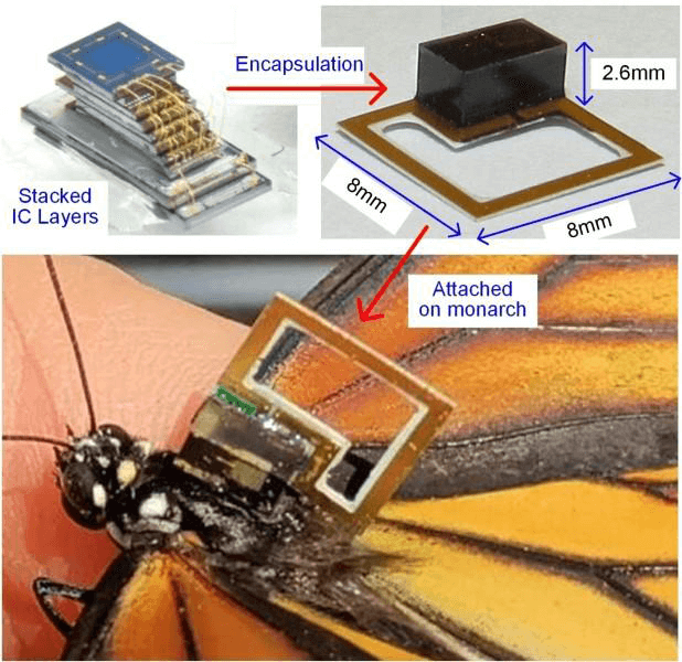
The sensor measures just 8x8x2.6mm, which includes an antenna and weighs just 62mg. The sensor can record various environmental factors, including temperature and light. The combination of this data, when used with a deep learning algorithm, can be used to infer the butterfly’s path. The new platform, called mSAIL, can be glued to the back of a Monarch butterfly while not hindering the butterfly’s ability to fly. The successful trial of the first sensor is now seeing the team manufacture 100 for use in a real-world trial.

Image courtesy University of Pittsburgh
How does this sensor demonstrate the advantage of stacked ICs?
To create such a tiny sensor, the researchers utilised stacked sensors connected together via bond wires. The staircase design allows for each chip layer to be connected to the one above and below it without needing special silicon vias or interconnectors, and this method of production is extremely cheap.
But the use of stacked ICs clearly demonstrates their advantage when it comes to increasing the complexity of an IC without needing to make transistors smaller. To double the number of transistors on a chip, either the chip needs to double in size or individual transistors need to shrink by 50%, but with transistors already in the 3nm scale, shrinking them further is extremely difficult. However, in the case of the butterfly sensor, using a larger piece of silicon is impractical as a large IC will be too big for the butterfly.
Instead, stacking chips vertically allows a device to retain its cross-sectional size while adding functionality. In the case of the butterfly, the stacking of ICs made the sensor taller, but this was not a problem for their application. This advantage will also be seen by modern electronic devices using chipsets and 3D stacked devices as it will allow for more transistors on a design without needing to reduce transistor sizes.
Stacked ICs are still in their infancy, but the push by major fabricators, including Intel and TSMC, for vertical technologies shows how their use will continue to grow and may even one day be the ideal method for increasing device complexity.

