Enhancing RF Sampling ADC Performance with Fully Differential Amplifiers
05-03-2025 | By Jack Pollard
Technical article by Srinivas Seshadri and Keyur Tejani of Texas Instruments
Higher data rates in wireless communication systems and the use of narrower pulses in radars to resolve close targets demand greater performance and bandwidth in test and measurement instruments. Radio-frequency (RF) test and measurement instruments, such as high-bandwidth oscilloscopes and RF digitizers, rely on RF sampling analog-to-digital converters (ADCs) that digitize signals from DC to multiple gigahertz.
RF sampling ADCs replace traditional mixer-based architectures followed by narrowband ADCs, reducing system complexity and improving the performance of wideband test and measurement instruments, radars, and wireless transceivers.
Traditionally, designers use a single-ended gain block in cascade with a passive balun to drive RF sampling ADCs. However, this approach has drawbacks that limit achievable performance. This article explores these challenges and illustrates how an RF fully differential amplifier (FDA) can enhance the performance of RF sampling ADCs.
DC-coupling RF sampling ADCs
RF sampling ADCs require differential inputs to reject common-mode noise, minimize interference, and improve second-order distortion. To achieve this, system designers often use transformer-based passive baluns to convert single-ended RF signals into differential signals.
However, passive baluns have a limited low-frequency range, typically operating from hundreds of kilohertz to tens of megahertz, depending on their bandwidth. This limitation affects the ability to digitize low-frequency signals in test and measurement applications.
The TRF1305 RF FDA offers a superior solution by performing single-ended to differential conversion with a large-signal bandwidth from DC to 6.5 GHz, while also providing gain. Figure 1 shows the TRF1305 RF FDA driving an RF sampling ADC in a DC-coupled application.
RF sampling ADCs have a narrow input common-mode range, and operation outside this range degrades ADC performance. The TRF1305 addresses this challenge by offering single or split flexible power supplies and output common-mode control, making it easier to match its output common mode to the ADC’s input common mode. These features make the amplifier well-suited for high-bandwidth oscilloscopes, arbitrary waveform generators, and RF digitizers.
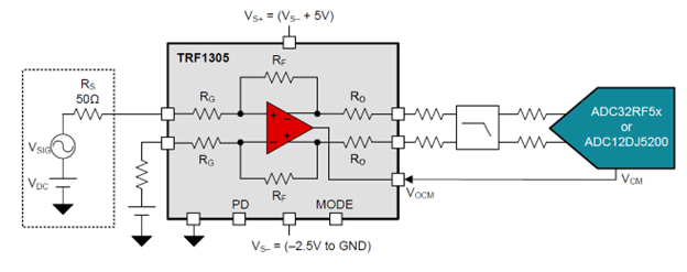
Figure 1. The TRF1305 RF FDA DC coupled to an RF sampling ADC
Improved Linearity
Nonlinearity in a signal chain impacts the detection of small signals in the presence of large interfering signals.
- In narrowband systems, second-order nonlinearity is typically filtered out as it falls outside the frequency band of interest.
- In wideband systems, however, second-order nonlinearity can fall within the signal band, making it impossible to filter out.
For example, an RF sampling ADC operating between 0.5 GHz and 2 GHz may experience second-order nonlinearity from a 0.5 GHz signal at 1 GHz (twice the frequency), which remains within the desired band.
To mitigate this issue:
- RF sampling ADCs are designed to minimize second-order nonlinearity when driven by balanced differential signals.
- Wideband passive baluns often introduce poor gain and phase imbalance, leading to unbalanced signaling and degraded ADC linearity.
- RF gain blocks used to amplify signals before passive baluns suffer from poor second-order nonlinearity due to their single-ended operation.
RF FDAs such as the TRF1305 and TRF1208 address these challenges by incorporating feedback techniques that improve gain and phase balance on the differential outputs. Their differential architecture minimizes second-order distortion, enhances system linearity, and provides signal amplification.
Protecting ADCs from damage
In test and measurement and aerospace and defense systems, the RF ADCs are often exposed to unknown and potentially high power levels. Since these ADCs are high-performance and expensive, it is crucial to protect them from damage due to overdrive conditions.
RF FDAs help protect ADCs by:
- Maintaining linearity while driving RF sampling ADCs to full scale.
- Limiting power during overload conditions through output clipping.
Figure 2 illustrates how the TRF1208 FDA saturates at 3.6 Vpp when overloaded with a continuous wave input at 4 GHz. With 16 dB of gain, the TRF1208’s output saturates at approximately 2 dBm of input power.
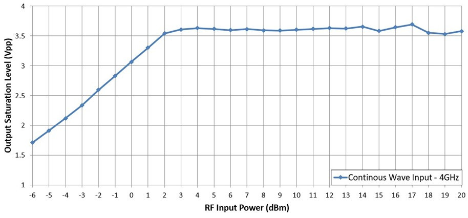
Figure 2. The differential output of the TRF1208 FDA clamps at 3.6 Vpp when overloaded with a continuous wave input at 4 GHz.
To further protect ADCs, an attenuator pad can be placed between the FDA and the ADC. This approach:
- Bounds the voltage swing at the ADC pins, preventing damage.
- Simplifies system design considerations.
- Provides additional design flexibility.
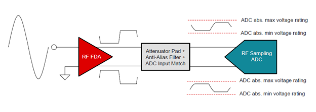
Figure 3. Output of RF FDA clips when overloaded, limiting signal power into the ADC.
Conclusion
The adoption of RF sampling ADCs simplifies the architecture of RF test and measurement instruments by reducing component count and board size.
RF FDAs, such as the TRF1305, further simplify system design by:
- Converting single-ended signals to differential over a wide bandwidth (DC to 6.5 GHz).
- Enhancing linearity to minimize second-order distortion.
- Protecting ADCs from potential damage due to overdrive.
By pairing wideband RF FDAs with RF sampling ADCs, engineers can achieve higher system performance, lower component count, reduced board size, and overall cost savings in RF test and measurement applications.
For more content like this, visit the Texas Instruments company blog.