Turning Nanowires into FETs for Next-Gen Electronics
13-03-2025 | By Liam Critchley
Key Things to Know:
- Miniaturization of FETs: Engineers are developing ultrathin silicon nanowires (below 30 nm) to create smaller and more efficient field-effect transistors (FETs) for advanced electronics.
- Challenges in Fabrication: Traditional lithography methods struggle with patterning nanoscale channels, limiting their application in large-area electronics like advanced displays.
- Breakthrough Growth Process: A new stepnecked catalytic growth method enables the creation of ultrathin silicon nanowires, improving electrostatic control and transistor performance.
- Enhanced Performance: The new FET design shows a significantly higher Ion/Ioff ratio and better gating efficiency, making it ideal for high-performance sensors and displays.
Field effect transistors (FETs) are common electrical components used in a lot of electronics today. With the miniaturization of many electronic devices becoming important for many tech products, engineers are also looking to miniaturize FETs. One way that this could be achieved is through nanowires, which are quasi-1D nanomaterials where electrons flow along one geometrical axis (along the length of the nanowire).
To coincide with conventional silicon-based technology, ultrathin silicon nanowires below 30 nm diameter have the potential to be used as channel materials for advanced and miniaturized FETs. For them to be feasible, they need to possess a strong electrostatic control with a short channel to enhance the driving current of the FET. Current fabrication methods for patterning the channels revolve around high-precision lithography, but it’s not applicable for large-area electronics―such as advanced displays. Researchers have now taken to using a metal-droplet-mediated catalytic growth approach to create silicon nanowires with a small diameter and short channel because the process is more versatile, cost-effective, and produces a higher manufacturing yield.
Developing Smaller FETs
FETs are specialist transistors that contain a source, drain and gate. FETs control the flow of current using an electric field through a semiconductor channel. When a voltage is applied to the gate, an electric field is generated to either attract or repel the charge carriers in the semiconductor channel―with the repel or attraction being dictated by the polarity of the voltage. This applied voltage controls the conductivity in the channel and governs the current flow of the channel between the source and drain terminals.
FETs allow electrons to flow along the channel in either direction, which enables FETs to be used for switching and amplifying signals―including multiplexing―for a range of devices, including motors and sensors. The bulkier the FET, the fewer transistors you can fit onto a chip, so either fewer signals can be amplified or the overall packaging will need to be larger. Because FETs are crucial for many electronic applications, fitting more FETs onto a chip not only allows for a higher power density but can also achieve it with a much smaller footprint that will help to further miniaturize electronic devices.
Scaling Down the Diameter of Nanowires
Achieving a greater electrostatic control and drive current in silicon nanowires requires the channels to be scaled down to below 30 nm diameter and the channel length to be shortened below 100 nm. Achieving this level of thinness and short channel length typically requires extreme ultraviolet (UV) or electron beam (e-beam) lithography. However, these are not compatible with large-area electronics and make it impossible to patten the channels and the source/drain with features below 100 nm.
Silicon nanowires with diameters below 30 nm have been fabricated using tiny metallic droplets as catalysts. This process is known as a vapour-liquid-solid (VLS) mechanism. However, VLS-grown silicon nanowires tend to form standing arrays, making it difficult to transfer and integrate the nanowires onto flat substrates that are used in large area electronic applications. E-beam lithography is also still the go-to technique for creating channels below 200 nm in length, which is a potential bottleneck for mass production of silicon nanowire-based FET devices.
Developing Ultrathin Nanowires for FET applications
Researchers have now developed a new approach for creating ultrathin and ultrashort silicon nanowires using a local-curvature-modulated catalytic growth process―which was based on a method from the group in previous research known as an in-plane solid-liquid-solid (IPSLS) growth mechanism. This process directs planar silicon nanowires and makes them ‘jump’ over a step edge, and during the jumping process, a catalytic droplet makes the nanowires undergo a stretching process over the step edge. The step edge was created onto the desired substrate using etching techniques to first get mini-steps that allow multiple nanowires to be fabricated, followed by etching a step edge in each of these mini-steps. This stretching process stretches the nanowires over the edge, making them thinner than the nanowires on either side of the step edge, creating very short segments of nanowires that have a strong gating effect that can be used as semiconducting channels.
Visualising the Step-Necking Growth Process
The following illustration provides a visual comparison between conventional fin-type field-effect transistor (finFET) structures and the newly developed step-necking catalytic growth technique. This comparison highlights the differences in fabrication methods and the resulting nanowire geometries, demonstrating how the innovative process enables the formation of ultrathin, short-channel silicon nanowires with enhanced gating properties.
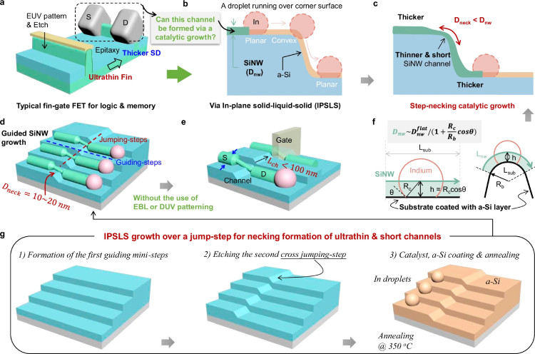
a Conventional fin-type field-effect transistor (finFET) with a narrow channel and wider source/drain (S/D) contacts, fabricated using extreme ultraviolet lithography (EUV). b, c Step-necking catalytic growth method, forming a distinct thick/thin/thick channel structure. d Guided growth of in-plane solid-liquid-solid (IPSLS) silicon nanowires (SiNWs) over a jumping step, creating necked SiNWs with <20 nm middle diameters and <100 nm channel lengths. e Short-channel FET using necked SiNWs, with the thin middle as the channel and thick ends as source/drain electrodes. f SiNWs grown over a convex edge exhibit a narrowed (necked) diameter (Dneck) when the bending track radius (Rb) matches the catalyst droplet size (Rc). g Step-by-step fabrication of step-necking SiNWs, including guiding step formation, etching, catalyst deposition, precursor coating, and annealing growth.
The process was inspired by the channel configuration in fin-gate FETs, where ultrashort silicon channels are sandwiched between bulkier source and drain contacts. In this process, the catalytic drop is precisely manipulated to deform during catalytic growth to modulate the diameter of the silicon nanowire, allowing ultrathin nanowires to be fabricated. This approach created nanowires with a thick/thin/thick short channel configuration directly onto a pre-coated and annealed amorphous silicon thin film.
Using this process, a silicon nanowire that possesses an original diameter of around 45 nm can be continuously narrowed down to less than 25 nm, with a narrow middle channel less than 100 nm in length. These thin and short channels are connected to the two thicker segments of nanowire at either end of the channel which acts as the source and drain electrodes.
Compared to FETs that are based on uniform channel silicon nanowires, the stepnecked FETs developed in this study showed a much higher Ion/Ioff ratio of 8 x10⁷ and a steeper subthreshold swing of 70 mV/dec. This is due to a stronger electrostatic gating in the middle of the thinner channel and improved source and drain contacts at the thicker ends of the nanowires.
This approach has shown that a scalable catalytic growth approach can be used as a deterministic fabrication method for crafting precise FET channels using silicon nanowires, with some of the key target applications being high-performance sensors and large-area displays.
Conclusion:
The development of ultrathin and ultrashort silicon nanowires through step-necking catalytic growth marks a significant advancement in the miniaturization of field-effect transistors (FETs). This innovative approach enables precise fabrication of nanoscale transistor channels with enhanced electrostatic control, leading to improved performance metrics such as a higher Ion/Ioff ratio and steeper subthreshold swing. By overcoming limitations in traditional lithography and integrating seamlessly with large-area electronics, this method paves the way for next-generation semiconductor devices. With potential applications in high-performance sensors and advanced display technologies, step-necked FETs could play a crucial role in the future of electronics, offering scalable and efficient solutions for the ever-growing demand for miniaturized, high-density circuits.
Reference: