Wafer-Scale LLM Chips: Faster, Smarter AI Processing
05-03-2025 | By Robin Mitchell
While GPUs and other shared-memory architectures have long been the backbone of modern AI applications, the relentless demand for greater computational power has spurred the exploration of wafer-scale solutions. Recently, researchers from the University of Edinburgh and Microsoft have pioneered a new approach to large language model (LLM) inference, harnessing wafer-scale integration to deliver massive parallelism. This breakthrough, known as WaferLLM, aims to push performance and energy efficiency well beyond the limits of conventional hardware.
Key Things to Know:
- Wafer-scale computing is redefining AI hardware: By integrating hundreds of thousands of cores onto a single chip, WaferLLM offers unprecedented computational power for large language models (LLMs).
- Overcoming GPU limitations: Traditional AI inference systems rely on GPUs, which struggle to efficiently utilise wafer-scale architectures. WaferLLM introduces novel parallel computing strategies to unlock higher performance.
- Breakthrough energy efficiency: WaferLLM is 22 times more energy-efficient than advanced GPUs, offering a more sustainable solution for AI inference in data centres.
- Future impact on AI and beyond: The principles behind WaferLLM could influence real-time analytics, scientific simulations, and edge computing, shaping the next generation of AI applications.
What challenges do wafer-scale technologies face, what exactly have the researchers developed to overcome these issues, and what are the implications of their wafer-scale LLM inference system for the future of AI and beyond?
The Challenges of Wafer Scale Technologies
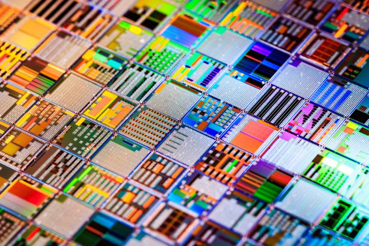
The evolution of integrated circuits has been nothing short of phenomenal, transforming the landscape of computing as we know it. From the humble beginnings of the first transistor to the current era of multi-core processors, the increase in transistor count and computing capabilities has been exponential. At the core of this advancement lies the concept of wafer-level integration, where an entire circuit is fabricated on a single silicon wafer. The significance of wafer-level integration cannot be overstated, as it has enabled the development of modern computing systems capable of handling complex tasks such as data processing and artificial intelligence.
How Wafer-Scale Computing Enables AI Innovation
Wafer-scale computing, however, takes this concept to the next level, integrating multiple dies onto a single wafer. This approach promises to unlock unprecedented levels of computing power, making it possible to handle massive tasks such as large-language models (LLMs) that are at the heart of modern AI systems. By integrating multiple dies onto a wafer, wafer-scale computing enables the creation of massive parallel computing systems, where each die can be programmed to perform a specific task.
When combined, these individual dies can perform complex tasks that would be impossible to accomplish with a single die, making wafer-scale computing an attractive option for next-generation AI systems. However, despite the promise of wafer-scale computing, numerous challenges must be addressed before it can be realised in practice.
Overcoming Data Communication Challenges in Wafer-Scale Systems
When multiple dies are integrated onto a single wafer, communication between dies becomes a significant challenge. Unlike traditional systems where data transfer occurs between chips connected through a bus or network, wafer-scale computing systems require dies to communicate with each other directly. This increased communication bandwidth leads to a significant increase in power consumption, which can result in overheating and reduced system stability. As a result, designing efficient communication systems between dies is crucial for achieving optimal performance in wafer-scale computing systems.
Manufacturing Complexities and Yield Challenges
Another critical challenge faced by wafer-scale integration is the increased complexity of manufacturing. Unlike traditional systems where individual dies are manufactured separately, wafer-scale computing involves the fabrication of multiple dies onto a single silicon wafer in a single manufacturing cycle. This not only increases the cost of manufacturing but also makes it more challenging to achieve high yield rates. If any part of the wafer is faulty, the entire wafer can become potentially unusable, resulting in significant losses.
Finally, the increased complexity of wafer-scale computing systems also poses significant challenges related to reliability and fault tolerance. As more dies are integrated onto a wafer, the likelihood of faults and errors increases, which can significantly impact the overall performance of the system.
University of Edinburgh and Microsoft Research Publish Paper on Wafer-Scale LIM Inference System
A new technical paper published by researchers from the University of Edinburgh and Microsoft has outlined their latest work on wafer-scale computing for LLMs. The paper, titled "WaferLLM: a Wafer-Scale LMM Inference System", outlines the researchers' development of a wafer-scale LLM system, called WaferLLM, and its capabilities compared to current LLM systems.
While wafer-scale computing presents an opportunity to vastly improve AI model inference speeds, its adoption requires significant advancements in software frameworks. The researchers behind WaferLLM acknowledge that traditional GPU-optimised LLM inference models struggle to take full advantage of wafer-scale hardware. By designing new parallel computing strategies, WaferLLM seeks to unlock higher efficiency and reduce energy overhead, potentially setting a new industry standard for large-scale AI computation.
How Wafer-Scale Computing Transforms AI Performance
Wafer-scale computing refers to the integration of hundreds of thousands of computing cores onto a single chip, which can significantly improve the performance of computing tasks. However, current LLM systems are designed to operate on shared memory architectures, such as GPUs, and are not optimised for wafer-scale architectures.
One of the key obstacles in wafer-scale computing is ensuring seamless communication across the vast number of cores. Unlike GPUs that rely on shared memory for coordination, wafer-scale architectures demand decentralised data handling techniques to prevent bottlenecks. WaferLLM introduces a novel approach to distributing computations, minimising latency and improving synchronisation across its extensive network of cores. This innovation could address a fundamental challenge in deploying wafer-scale AI accelerators at scale.
To address this issue, the researchers developed a novel PLMR device (Parallel Logic Matrix Router) model that captures the unique characteristics of wafer-scale accelerators, including their large distributed on-chip memories and ultra-high on-chips memory bandwidth. This model was then used to guide the development of WaferLLM, a wafer-scale LMM inference system that is designed to fully exploit the capabilities of wafer-scale accelerations.
Reducing AI’s Energy Footprint with Wafer-Scale Innovation
In addition to enhancing raw computational performance, WaferLLM also contributes to AI sustainability by reducing energy consumption per inference task. With data centres facing mounting pressure to limit power usage, wafer-scale AI accelerators may serve as a more energy-efficient alternative to conventional GPU-based clusters. By optimising data flow through its ultra-high-bandwidth on-chip memory, WaferLLM has the potential to significantly cut down operational costs for large-scale AI deployments.
According to the researchers, WaferLLM achieves a significant improvement in performance compared to current LLM inference systems. Specifically, WaferLLM is able to deliver 606 times faster and 22 times more energy-efficient GEM (Generalised Eigenvector Matrix) operations compared to an advanced GPU, and 39 times faster decoding with 1,7 times better energy efficiency.
Scalability Advantages of WaferLLM for LLMs
The research team also highlighted how WaferLLM’s architecture allows for more predictable scaling of LLM inference workloads. Unlike traditional GPUs, which experience diminishing efficiency returns when adding more compute units, wafer-scale accelerators can maintain linear performance improvements due to their unified hardware design. This feature makes them particularly suitable for handling increasingly complex AI models, such as multi-modal learning systems that integrate text, image, and audio processing.
The researchers also evaluated WaferLLM on a commodity wafer-scale accelerometer and found that it was able to deliver 200 times better wafer-scale accelerator utilisation than state-of-the-art LLM inference systems.
Beyond LLM inference, WaferLLM’s foundational principles could influence the next generation of AI hardware, particularly in fields like real-time analytics, scientific simulations, and edge computing. As AI applications demand ever-larger models and datasets, the ability to perform inference with minimal latency and reduced power draw will be crucial in shaping the future of AI deployment strategies.
The Road Ahead For Wafer-Scale Artificial Intelligences
Wafer-scale parts promise to revolutionise AI and data analysis, offering unprecedented computational density that will power new frontiers in both automation and research. However, in order for such technologies to become a reality, engineers will need to develop specialised skills in thermal management, as well as ultra-efficient communication structures and fault-tolerant designs, to harness the full potential of these single-die advances while navigating increasingly complex manufacturing demands.
Even though this technology could alleviate bottlencks in LLM inference and training, concerns surrounding power consumption and yield losses introduce unique sustainability and reliability issues. As wafer-scale systems redefined performance benchmarks, collaborations between academia, industry, and the AI community will likely accelerate breakthroughs, but may also prompt regulatory discussions on ensuring the safe and equitable implementation.
In the long run, wafer-scale solutions may drive disruptive innovation in robotics and healthcare, enabling massive-scale AI that has a direct impact on everyday life and global industries.
